Over the last number of weeks I have been tearing down and performing research into a device powered by an STM32F103x microcontroller. As this particular device had RDP (Read-Out Protection) set to Level 1 it was not possible to dump the firmware from the device. This meant any attempts to inspect the contents of the flash via debugger would generate an immediate HF (Hard Fault).
While searching for workarounds, I came across a paper by Johannes Obermaier and Stefan Tatschner titled “Shedding too much Light on a Microcontroller’s Firmware Protection”. Although the paper covers a number of attacks on the STM32, one piqued my interest. This attack, under “3.3 Debug Interface Exploit” of the paper linked to above, exploits a race condition between the SWD debug interface and the enforcement of the readout protection. This allowed the authors to extract the firmware from a read protected STM32F0 a word at a time.
Now, I’m not able to do this attack, nor the paper, any justice here, so I would recommend reading the full paper. It’s a fantastic read.
From here I was left with a problem: I had no idea about any of the SWD inner workings; all I knew was that it was exposed on the STM32F103x I was targeting, that it was a ‘two wire’ debug interface, and that I could use OpenOCD to interrogate it. This said, the authors of the paper above did release a working exploit, but where’s the fun in running a exploiting something if you don’t understand how it works, eh? :)
As a result of all of this, I have spent many evenings poring over datasheets in order to better understand SWD, and build my own SWD client implementation in Python. The intention being to both better understand the protocol, and also provide an easily extensible set of modules which may be used in further research.
So, with all of this said…
Down the rabbit hole.

This series of posts will detail my encounters with SWD, specifically: how the protocol functions, notable caveats, and how to bend it to your will. As these posts have been compiled by collating notes, there may be errors present. If you see any problems please reach out and I will ensure they are corrected - with credit, of course! :)
Finally, a quick disclaimer as to the content of these posts:
Before acting on any information below, you should ensure that all parameters have been validated against the official documentation before use! Failure to do so could lead to device damage, and will most certainly lead to undefined behaviour.
SWD?
Serial Wire Debug (SWD) is an alternate debugging interface to JTAG. This interface can be used, with an appropriate debugger, to perform a number of useful operations, such as:
- Debug microprocessor cores (MCUs) attached to the system.
- This includes display and modification of registers and memory.
- Debug components that exist WITHIN a System On Chip (SoC).
- Provides access to debug components with no directly exposed pins.
- This assumes that the component is connected to a debug bus internally.
- Access JTAG interfaces of devices attached to the system.
- This requires an appropriate
JTAG-APAccess Port (AP).
- This requires an appropriate
This post is written regarding SWD as it exists in ADI v5 (ARM Debug Interface), per ARM IHI 0031C.
Lines
Unlike JTAG, SWD only requires two lines for operation: SWDIO and SWDCLK.
SWDIO- I/O- This is driven by both the host AND the target, depending on dataflow.
- When the host controls the line, bits are banged onto this wire on the falling edge of the clock.
- When the target controls the line, bits are banged onto this wire on the rising edge of the clock.
SWCLK- Clock- Provides clocking of the debug interface.
- This is driven by the host.
The comments related to the rising or falling edge of the clock may be better explained by the following diagram:
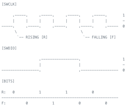
For context, let’s assume that the host has just written a request packet onto
SWDIO. Let’s also assume that the above ‘capture’ is taken after this
request has already been written, and control of SWDIO has been transferred
to the target. Now, don’t worry too much about the terminology yet, I will go
into more detail on this later, just be aware that the host has REQUESTed
something from the target.
In this case, the host would read a response of 0b0110 from the target.
If the above scenario were reversed, and this capture was of target reading a
REQUEST from the host, the value on SWDIO would be read by the target as
0b0100.
Bit Order
An important caveat to note when working with SWD - per section 4.2.4 of ARM IHI 0031C:
All data values in SWD operations are transferred LSB first.
As a result of this, data on the SWDIO line will appear to be backwards if
read with a debugger which doesn’t automatically flip the bit order; meaning
that the least significant bit (LSB) will be placed on the wire FIRST,
instead of last.
In order to better explain, consider the following example:
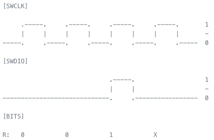
The last clock cycle is being ignored here (hence the X), as in this context
it would be interpreted as a turnround sequence by the host. This will be
covered later, but this is why we’re only interpreting THREE bits when there
are four in the diagram! :)
In line with the above diagram, and assuming that this was an SWD ACK packet
written onto SWDIO by the target, a value of 0b001 would be read by the
host. If taken at face value, and as it appeared on the wire, this response
would indicate an SWD ACK OK (0b001) was being sent in response to our
most recent request. However…
THIS IS NOT THE CASE, THE RESPONSE IS ACTUALLY AN SWD ACK FAULT (0b100).
This is due to all data on the wire being represented in LSB order. In order to flip - so that the most significant bit (MSB) is first - simply reverse the order of the bits:
0b001becomes0b1000b100becomes0b001- …et cetera
DP vs AP vs DAP?!
Before we continue, we should clarify a few terms used heavily throughout, namely port types:
- Debug Port (DP).
- The interface to which the debugger is physically connected.
- Provides external access to the system.
- Access Port (AP).
- Exist within the system and are accessed externally via a Debug Port (
DP). - Though there may be more, there WILL be at least one
APin given system. - The
APto interact with is specified via theAPSELvalue in theDPSELECTregister.
- Exist within the system and are accessed externally via a Debug Port (
- Debug Access Port (DAP).
APandDP.
The placement, and differences between these ports, may be better explained by the following diagram:
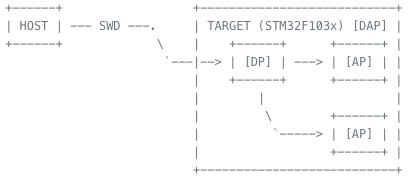
In the above diagram, SWD represents the SWD protocol being spoken over a
set of two wires.
Packets
Data transfers in SWD are ‘packet’ based, and successful requests will consist of three components:
- 8-bits - Request Header.
- Sent from the host-to-target
- 3-bits - An Acknowledgement (ACK).
- Sent from the target to the host.
- 33-bits - A Payload.
- 32-bits for data, and 1-bit for parity.
- This may be host-to-target in the case of a write.
- This may be target-to-host in the case of a read.
All together a request will be 46 bits long, with one bit per clock cycle.
Those with a keen eye will note that there are only 44-bits accounted for in
the list above, rather than 46. This is due to 2-bits being used for the two
turnround sequences required to transfer control of the SWDIO line
between the host and target.
These turnround sequences would be inserted in slightly different places depending on whether this was a read or write request:
- Read
- One ‘turn round’ would be inserted after the request header is written.
- One ‘turn round’ would be inserted after the payload is written.
- Write
- One ‘turn round’ would be inserted after the request header is written.
- One ‘turn round’ would be inserted after the ACK is written.
This sequence is needed to transfer control of the SWDIO
line between host and target as SWDIO being driven
by either host or target. The turnround sequence is used to yield control and
avoid both host and target attempting to write to SWDIO simultaneously
(which would cause contention).
One caveat to note here is that in the case of a request failure, the payload may be omitted and only the ACK returned.
Request Header
The request header has a very simple and fixed format. It is 8-bits long, and
instructs the target whether the request is being made to read or to write to
it, whether it is intended for an AP or DP, and the address of the target
register.
The format of a request packet header is as follows - per section 4.3 of ARM IHI 0031C:
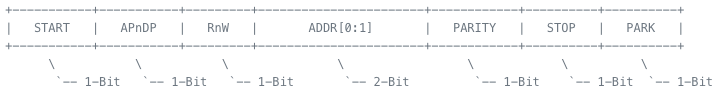
START- This should always be high (
0b1).
- This should always be high (
APnDP- High (
0b1) for access toAPaccess. - Low (
0b0) forDPaccess.
- High (
RnW- High (
0b1) for READ access. - Low (
0b0) for WRITE access.
- High (
ADDR[0:1]- Two bits representing the register to access.
- This address is once again written to
SWDIOLSB first!
PARITY- In the case of a request packet, this field is high (
0b1) if the number of high (0b1) bits in theAPnDP,RnW, andADDRfields combined is odd. Low (0b0) if an even.
- In the case of a request packet, this field is high (
STOP- This should always be low (
0b0).
- This should always be low (
PARK- This should always be high (
0b1).
- This should always be high (
Consider the following examples:
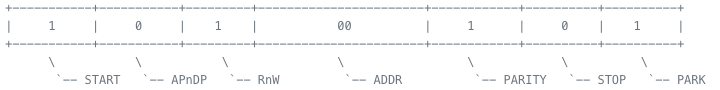
This above would indicate a READ request of the DP IDR register
(0b00).
This would indicate a WRITE request to the DP SELECT register (0b10).
Once again, the ADDR of the SELECT register is LSB first, so 0b10
becomes 0b01 on the wire.
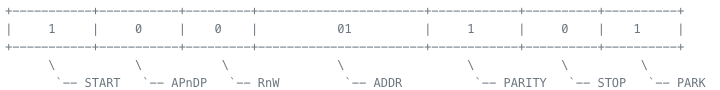
Acknowledgement (ACK)
The format of an ACK is as follows - per section 4.3 of ARM IHI 0031C:
The mapping of valid responses of an ACK are as follows:
OK(0b001)- “Everything’s fine.”
- This will appear on the wire LSB first (
0b100).
WAIT(0b010)- “Try again in a bit, I’m busy.”
- This will appear on the wire LSB first (
0b010).
FAULT(0b100)- “Something went wrong.”
- This will appear on the wire LSB first (
0b001).
One caveat for the FAULT response is that when a DP has responded with
this result, the DP will only then reply to:
READof theDPIDPregister.- Used to identify the device.
READof theDPCTRL/STATregister.- Used to read the status bits which may indicate cause of failure.
WRITEof theDPABORTregister.- Used to reset status bits, clearing the fault.
Payload
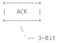
The logical mapping inside of the payload will differ depending on the type of request, however both read and write payloads look the same on the wire from a conceptual standpoint. This format is as follows - per section 4.3 of ARM IHI 0031C:
RDATA and WDATA in this diagram simply refers to DATA in a read or write
context - respectively. This is only used here to demonstrate that the payload
occupies the same space for both read and write operations.
Finally, the parity calculation used to populate the parity bit is performed
in the same way as the request header. If the number of bits in the DATA
field that are high (0b1) is odd, this parity bit will be high (0b1). If
even, the parity bit will be low (0b0).
FIN.
…Phew! Okay, that’s enough overview for now. Although this post has been very dry, it should make the next much easier. The next post should contain information related to interacting with SWD via an FT2232H via Python, and how to ‘map’ the DAP from SWD.
Hopefully I’ll have some PoC code ready to go, too!
Thanks
Cheers to @SiouxDenim and @AgustinGianni for proofreading this post and correcting my terrible grammar.